
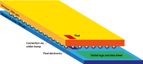
Current pixel detector technologies (see figures for the two main approaches) capable of high rates such as those employed by the LHC experiments ATLAS and CMS or the PILATUS and EIGER detectors for X-rays at synchrotron radiation sources are built in a hybrid technology consisting of a passive sensor bump-bonded to an active read-out chip.
This approach has the disadvantages of high cost and large amounts of (heavy) material, which disqualifies it for tracking low momentum particles. Established monolithic pixel technologies (such as the MIMOSA detectors employed by the STAR experiment at RHIC) on the other hand collect charges via diffusion and are thus too slow for high rate applications.
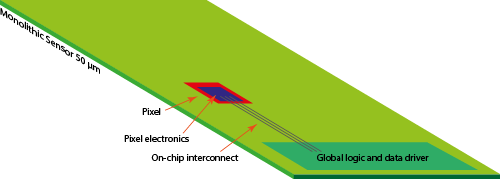
The novel High Voltage Monolithic Active Pixel Sensors (HV-MAPS) developed by Ivan Perić (Karlsruhe Institute of Technology, KIT, formerly ZITI, Heidelberg University) use a commercial CMOS process qualified for “high” voltages up to 120 V. This allows fast collection of charges via drift whilst at the same time integrating the read-out electronics on the same die. As the active region is very thin, the sensors can be thinned to below 50 μm. This makes HV-MAPS ideally suited for tracking low momentum particles at very high rates.
In close collaboration with the Mu3e group at the physics institute in Heidelberg and Ivan Perić, we have characterized a series of prototype HV-MAPS sensors, both in the respective labs and in test beam campaigns at CERN, DESY and MAMI in Mainz.